Pentium 4
 | |
| General information | |
|---|---|
| Launched | November 20, 2000 |
| Discontinued | December 7, 2007 (orders) [1] August 8, 2008 (shipments) [2] |
| Marketed by | Intel |
| Designed by | Intel |
| Common manufacturer |
|
| Performance | |
| Max. CPU clock rate | 1.3 GHz to 3.8 GHz |
| FSB speeds | 400 MT/s to 1066 MT/s |
| Cache | |
| L1 cache | 16 KB (8 KB data + 8 KB instructions) |
| L2 cache | Up to 2 MB |
| L3 cache | 2 MB (Gallatin only) |
| Architecture and classification | |
| Microarchitecture | NetBurst |
| Instruction set | x86 (i386), x86-64 (only some chips) |
| Instructions | MMX, SSE, SSE2, SSE3 (since Prescott) |
| Physical specifications | |
| Transistors |
|
| Sockets | |
| Products, models, variants | |
| Brand names |
|
| History | |
| Predecessor | Pentium III |
| Successors |
|
| Support status | |
| Unsupported | |
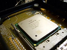
Pentium 4[3][4] is a series of single-core CPUs for desktops, laptops and entry-level servers manufactured by Intel. The processors were shipped from November 20, 2000 until August 8, 2008.[5][6] All Pentium 4 CPUs are based on the NetBurst microarchitecture, the successor to the P6.
The Pentium 4 Willamette (180 nm) introduced SSE2, while the Prescott (90 nm) introduced SSE3 and later 64-bit technology. Later versions introduced Hyper-Threading Technology (HTT). The first Pentium 4-branded processor to implement 64-bit was the Prescott (90 nm) (February 2004), but this feature was not enabled. Intel subsequently began selling 64-bit Pentium 4s using the "E0" revision of the Prescotts, being sold on the OEM market as the Pentium 4, model F. The E0 revision also adds eXecute Disable (XD) (Intel's name for the NX bit) to Intel 64. Intel's official launch of Intel 64 (under the name EM64T at that time) in mainstream desktop processors was the N0 stepping Prescott-2M.
Intel also marketed a version of their low-end Celeron processors based on the NetBurst microarchitecture (often referred to as Celeron 4), and a high-end derivative, Xeon, intended for multi-socket servers and workstations. In 2005, the Pentium 4 was complemented by the more advanced dual-core-brands Pentium D and Pentium Extreme Edition, all were succeeded at the top range by the Core 2 brand, while production continued until 2008,[7] with Pentium 4 replaced by Pentium Dual-Core.[8]
Microarchitecture
[edit]This section needs additional citations for verification. (March 2021) |
In benchmark evaluations, the advantages of the NetBurst microarchitecture were unclear. With carefully optimized application code, the first Pentium 4s outperformed Intel's fastest Pentium III (clocked at 1.13 GHz at the time), as expected. But in legacy applications with many branching or x87 floating-point instructions, the Pentium 4 would merely match or run slower than its predecessor. Its main downfall was a shared unidirectional bus. The NetBurst microarchitecture consumed more power and emitted more heat than any previous Intel or AMD microarchitectures.
As a result, the Pentium 4's introduction was met with mixed reviews: Developers disliked the Pentium 4, as it posed a new set of code optimization rules. For example, in mathematical applications, AMD's lower-clocked Athlon (the fastest-clocked model was clocked at 1.2 GHz at the time) easily outperformed the Pentium 4, which would only catch up if software was re-compiled with SSE2 support. Tom Yager of Infoworld magazine called it "the fastest CPU – for programs that fit entirely in cache". Computer-savvy buyers avoided Pentium 4 PCs due to their price premium, questionable benefit, and initial restriction to Rambus' RDRAM.[9][10][11] In terms of product marketing, the Pentium 4's singular emphasis on clock frequency (above all else) made it a marketer's dream.[12] The result of this was that the NetBurst microarchitecture was often referred to as a marchitecture[13] by various computing websites and publications during the life of the Pentium 4. It was also called "NetBust",[14][13] a term popular with reviewers who reflected negatively upon the processor's performance.
The two classical metrics of CPU performance are instructions per cycle (IPC) and clock speed. While IPC is difficult to quantify due to dependence on the benchmark application's instruction mix, clock speed is a simple measurement yielding a single absolute number. Unsophisticated buyers would simply consider the processor with the highest clock speed to be the best product, and the Pentium 4 had the fastest clock speed. Because AMD's processors had slower clock speeds, it countered Intel's marketing advantage with the "megahertz myth" campaign. AMD product marketing used a "PR-rating" system, which assigned a merit value based on relative performance to a baseline machine.
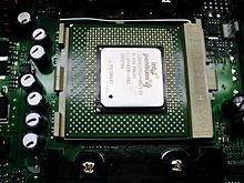
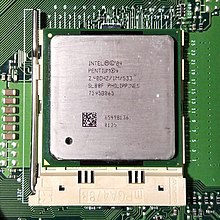

At the launch of the Pentium 4, Intel stated that NetBurst-based processors were expected to scale to 10 GHz[15] after several fabrication process generations. However, the clock speed of processors using the NetBurst microarchitecture reached a maximum of 3.8 GHz. Intel had not anticipated a rapid upward scaling of transistor power leakage that began to occur as the die reached the 90 nm lithography and smaller. This new power leakage phenomenon, along with the standard thermal output, created cooling and clock scaling problems as clock speeds increased. Reacting to these unexpected obstacles, Intel attempted several core redesigns (Prescott most notably) and explored new manufacturing technologies, such as using multiple cores, increasing FSB speeds, increasing the cache size, and using a longer instruction pipeline along with higher clock speeds.
The code cache was replaced by a trace cache which contained decoded microoperations rather than instructions with advantage of eliminating instruction decoding bottleneck so that the design can use RISC technology.[16]: 48 This came with a disadvantage of less compact cache taking up more chip space and consuming power.[16]: 48
These solutions failed, and from 2003 to 2005, Intel shifted development away from NetBurst to focus on the cooler-running Pentium M microarchitecture. On January 5, 2006, Intel launched the Core processors, which put greater emphasis on energy efficiency and performance per clock cycle. The final NetBurst-derived products were released in 2007, with all subsequent product families switching exclusively to the Core microarchitecture.[citation needed]
Testing and validation
[edit]According to Bob Bentley, presenting on behalf of Intel at the 38th annual Design Automation Conference, "The microarchitecture of the Pentium 4 processor is significantly more complex than any previous IA-32 microprocessor, so the challenge of validating the logical correctness of the design in a timely fashion was indeed a daunting one." He hired a team of 60 recent graduates to help with testing and validation.[17]
Processor cores
[edit]| Desktop | Laptop | ||||
|---|---|---|---|---|---|
| Code-named | Node | Release date | Code-named | Node | Release date |
| Willamette Northwood Prescott |
180 nm 130 nm 90 nm |
Nov 2000 Jan 2002 Mar 2004 |
Northwood | 130 nm | Jun 2003 |
| Northwood Pentium 4-M |
130 nm | Mar 2002 | |||
| Hyper-threading (HT) | |||||
| Northwood Prescott Prescott 2M Cedar Mill |
130 nm 90 nm 90 nm 65 nm |
Nov 2002 Feb 2004 Feb 2005 Jan 2006 |
Northwood Prescott |
130 nm 90 nm |
Sep 2003 Jun 2004 |
| Gallatin XE Prescott 2M XE |
130 nm 90 nm |
Sep 2003 Feb 2005 |
|||
| List of Intel Pentium 4 processors | |||||
Pentium 4 processors have an integrated heat spreader (IHS) that prevents the die from accidentally being damaged when mounting and unmounting cooling solutions. Prior to the IHS, a CPU shim was some times used by people worried about damaging the core. Overclockers sometimes removed the IHS from Socket 423 and Socket 478 chips to allow for more direct heat transfer. On Socket 478 Prescott processors and processors using the Socket LGA 775 (Socket T) interface, the IHS is directly soldered to the die or dies, making it difficult to remove.
Willamette
[edit]
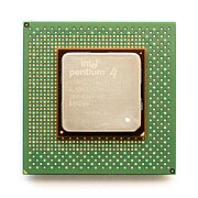

Willamette, the project codename for the first NetBurst microarchitecture implementation, experienced long delays in the completion of its design process. The project was started in 1998, when Intel saw the Pentium II as their permanent line. At that time, the Willamette core was expected to operate at frequencies up to about 1 GHz. However, the Pentium III was released while Willamette was still being finished. Due to the radical differences between the P6 and NetBurst microarchitectures, Intel could not market Willamette as a Pentium III, so it was marketed as the Pentium 4.
On November 20, 2000, Intel released the Willamette-based Pentium 4 clocked at 1.4 and 1.5 GHz. Most industry experts regarded the initial release as a stopgap product, introduced before it was truly ready. According to these experts, the Pentium 4 was released because the competing Thunderbird-based AMD Athlon was outperforming the aging Pentium III, and further improvements to the Pentium III were not yet possible.[citation needed] This Pentium 4 was produced using a 180 nm process and initially used Socket 423 (also called socket W, for "Willamette"), with later revisions moving to Socket 478 (socket N, for "Northwood"). These variants were identified by the Intel product codes 80528 and 80531 respectively.
On the test bench, the Willamette was somewhat disappointing to analysts in that not only was it unable to outperform the Athlon and the highest-clocked Pentium IIIs in all testing situations, but it was not superior to the budget segment's AMD Duron.[18] Although introduced at prices of $644 (1.4 GHz) and $819 (1.5 GHz) for 1000 quantities to OEM PC manufacturers[citation needed] (prices for models for the consumer market varied by retailer), it sold at a modest but respectable rate, handicapped somewhat by the requirement for relatively fast yet expensive Rambus Dynamic RAM (RDRAM). The Pentium III remained Intel's top selling processor line, with the Athlon also selling slightly better than the Pentium 4. While Intel bundled two RDRAM modules with each boxed Pentium 4, it did not facilitate Pentium 4 sales and was not considered a true solution by many.
In January 2001, a still slower 1.3 GHz model was added to the range, but over the next twelve months, Intel gradually started reducing AMD's leadership in performance. In April 2001 a 1.7 GHz Pentium 4 was launched, the first model to provide performance clearly superior to the old Pentium III. July saw 1.6 and 1.8 GHz models and in August 2001, Intel released 1.9 and 2 GHz Pentium 4s. In the same month, they released the 845 chipset that supported much cheaper PC133 SDRAM instead of RDRAM.[19] The fact that SDRAM was so much cheaper caused the Pentium 4's sales to grow considerably.[19] The new chipset allowed the Pentium 4 to quickly replace the Pentium III, becoming the top-selling mainstream processor on the market.
The Willamette code name is derived from the Willamette Valley region of Oregon, where a large number of Intel's manufacturing facilities are located.[citation needed]
Northwood
[edit]
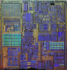
In January 2002, Intel released Pentium 4s with a new core codenamed Northwood at speeds of 1.6 GHz, 1.8 GHz, 2 GHz and 2.2 GHz.[20][21] Northwood (product code 80532) combined an increase in the L2 cache size from 256 KB to 512 KB (increasing the transistor count from 42 million to 55 million) with a transition to a new 130 nm fabrication process.[21] Making the processor out of smaller transistors means that it can run at higher clock speeds and produce less heat. In the same month boards utilizing the 845 chipset were released with enabled support for DDR SDRAM which provided double the bandwidth of PC133 SDRAM, and alleviated the associated high costs of using Rambus RDRAM for maximal performance with Pentium 4.[citation needed]
A 2.4 GHz Pentium 4 was released on April 2, 2002, and the bus speed increased from 400 MT/s to 533 MT/s (133 MHz physical clock) for the 2.26 GHz, 2.4 GHz, and 2.53 GHz models in May, 2.66 GHz and 2.8 GHz models in August, and 3.06 GHz model in November. With Northwood, the Pentium 4 came of age. The battle for performance leadership remained competitive (as AMD introduced faster versions of the Athlon XP) but most observers agreed that the fastest-clocked Northwood-based Pentium 4 was usually ahead of its rival.[citation needed] This was particularly so in mid-2002, when AMD's changeover to its 130 nm production process did not help the initial "Thoroughbred A" revision Athlon XP CPUs to clock high enough to overcome the advantages of Northwood in the 2.4 to 2.8 GHz range.[22]
The 3.06 GHz Pentium 4 enabled Hyper-Threading Technology that was first supported in Foster-based Xeons. This began the convention of virtual processors (or virtual cores) under x86 by enabling multiple threads to be run at the same time on the same physical processor. By shuffling two (ideally differing) program instructions to simultaneously execute through a single physical processor core, the goal is to best utilize processor resources that would have otherwise been unused from the traditional approach of having these single instructions wait for each other to execute singularly through the core. This initial 3.06 GHz 533FSB Pentium 4 Hyper-Threading enabled processor was known as Pentium 4 HT and was introduced to mass market by Gateway in November 2002.
On April 14, 2003, Intel officially launched the new Pentium 4 HT processor. This processor used an 800 MT/s FSB (200 MHz physical clock), was clocked at 3 GHz, and had Hyper-Threading technology.[23] This was meant to help the Pentium 4 better compete with AMD's Opteron line of processors. Meanwhile, with the launch of the Athlon XP 3200+ in AMD's desktop line, AMD increased the Athlon XP's FSB speed from 333 MT/s to 400 MT/s, but it was not enough to hold off the new 3 GHz Pentium 4 HT.[24]
The Pentium 4 HT's increase to a 200 MHz quad-pumped bus (200 x 4 = 800 MHz effective) greatly helped to satisfy the bandwidth requirements the NetBurst architecture desired for reaching optimal performance. While the Athlon XP architecture was less dependent on bandwidth, the bandwidth numbers reached by Intel were well out of range for the Athlon's EV6 bus. Hypothetically, EV6 could have achieved the same bandwidth numbers, but only at speeds unreachable at the time. Intel's higher bandwidth proved useful in benchmarks for streaming operations[citation needed], and Intel marketing wisely capitalized on this as a tangible improvement over AMD's desktop processors[citation needed]. Northwood 2.4 GHz, 2.6 GHz and 2.8 GHz variants were released on May 21, 2003. A 3.2 GHz variant was launched on June 23, 2003 and the final 3.4 GHz version arrived on February 2, 2004.
Overclocking early stepping Northwood cores yielded a startling phenomenon. While core voltage approaching 1.7 V and above would often allow substantial additional gains in overclocking headroom, the processor would slowly (over several months or even weeks) become more unstable over time with a degradation in maximum stable clock speed before dying and becoming totally unusable. This became known as Sudden Northwood Death Syndrome (SNDS), which was caused by electromigration.[25]
Pentium 4 M
[edit]Also based on the Northwood core, the Mobile Intel Pentium 4 Processor - M[26] (also known as the Pentium 4 M) was released on April 23, 2002, and included Intel's SpeedStep and Deeper Sleep technologies. Its TDP is about 35 watts in most applications. This lowered power consumption was due to lowered core voltage, and other features mentioned previously.
Unlike the desktop Pentium 4, the Pentium 4 M did not feature an integrated heat spreader (IHS), and it operates at a lower voltage. The lower voltage means lower power consumption, and in turn less heat. However, according to Intel specifications, the Pentium 4 M had a maximum thermal junction temperature rating of 100 degrees C, approximately 40 degrees higher than the desktop Pentium 4.
Mobile Pentium 4
[edit]The Mobile Intel Pentium 4 Processor[27] was released to address the problem of putting a full desktop Pentium 4 processor into a laptop, which some manufacturers were doing[citation needed]. The Mobile Pentium 4 used a 533 MT/s FSB, following the desktop Pentium 4's evolution. Oddly, increasing the bus speed by 133 MT/s (33 MHz) caused a massive increase in TDPs, as mobile Pentium 4 processors emitted 59.8–70 W of heat, with the Hyper-Threading variants emitting 66.1–88 W. This allowed the mobile Pentium 4 to bridge the gap between the desktop Pentium 4 (up to 115 W TDP), and the Pentium 4 M (up to 35 W TDP).
Intel's naming conventions made it difficult at the time of the processor's release to identify the processor model. There was the Pentium III mobile chip, the Pentium 4 M, the Mobile Pentium 4, and then the Pentium M, which itself was based on the Pentium III and was significantly faster and more power-efficient than the former three.
Northwood (Extreme Edition)
[edit]In September 2003, at the Intel Developer Forum, the Pentium 4 Extreme Edition (P4EE) was announced, just over a week before the launch of Athlon 64 and Athlon 64 FX. The design was mostly identical to Pentium 4 (to the extent that it would run in the same motherboards), but differed by an added 2 MB of level 3 cache. It shared the same Gallatin core as the Xeon MP, though in a Socket 478 form factor (as opposed to Socket 603 for the Xeon MP) and with an 800 MT/s bus, twice as fast as that of the Xeon MP.

While Intel maintained that the Extreme Edition was aimed at gamers, critics viewed it as an attempt to steal the Athlon 64's launch thunder, nicknaming it the "Emergency Edition".[28] With a price tag of $1000, it was also referred to as the "Expensive Edition" and "Extremely Expensive".[29]
The added cache generally resulted in a noticeable performance increase in most processor intensive applications. Multimedia encoding and certain games benefited the most, with the Extreme Edition outperforming the Pentium 4, and even the two Athlon 64 variants, although the lower price and more balanced performance of the Athlon 64 (particularly the non-FX version) led to it usually being seen as the better value proposition. Nonetheless, the Extreme Edition did achieve Intel's apparent aim, which was to prevent AMD from being the performance champion with the new Athlon 64, which was winning every single major benchmark over the existing Pentium 4s.
In January 2004, a 3.4 GHz version was released for Socket 478, and in Summer 2004 the CPU was released using the new Socket 775 (LGA 775). A slight performance increase was achieved in late 2004 by increasing the bus speed from 800 MT/s to 1066 MT/s, resulting in a 3.46 GHz Pentium 4 Extreme Edition. By most metrics, this was on a per-clock basis the fastest single-core NetBurst processor that was ever produced, even outperforming many of its successor chips (not counting the dual-core Pentium D). Afterwards, the Pentium 4 Extreme Edition was migrated to the Prescott core. The new 3.73 GHz Extreme Edition had the same features as a 6x0-sequence Prescott 2M, but with a 1066 MT/s bus. In practice however, the 3.73 GHz Pentium 4 Extreme Edition almost always proved to be slower than the 3.46 GHz Pentium 4 Extreme Edition, which is most likely due to the lack of an L3 cache and the longer instruction pipeline. The only advantage the 3.73 GHz Pentium 4 Extreme Edition had over the 3.46 GHz Pentium 4 Extreme Edition was the ability to run 64-bit applications since all Gallatin-based Pentium 4 Extreme Edition processors lacked the Intel 64 (then known as EM64T) instruction set.
Although never a particularly good seller, especially since it was released in a time when AMD was asserting near total dominance in the processor performance race, the Pentium 4 Extreme Edition established a new position within Intel's product line, that of an enthusiast oriented chip with the highest-end specifications offered by Intel chips, along with unlocked multipliers to allow for easier overclocking. In this role it has since been succeeded by the Pentium Extreme Edition (The Extreme version of the dual-core Pentium D), the Core 2 Extreme, the Core i7 and the Core i9.
Contrary to popular belief, however, the Socket 478 versions of the Pentium 4 Extreme Edition CPUs such as the Gallatin-based Pentium 4 Extreme Edition for Socket 478 all have a locked multiplier, meaning that they are not overclockable unless the front-side bus speeds are increased (which runs the potential risks of erratic behaviors such as reliability and stability issues). Only the Socket 775/LGA 775 versions of the Pentium 4 Extreme Edition, as well as the Pentium Extreme Edition (Smithfield) and Engineering Sample CPUs have unlocked multipliers.
Prescott
[edit]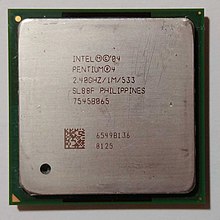

On February 1, 2004, Intel introduced a new core codenamed Prescott. The core used the 90 nm process for the first time, which one analyst described as "a major reworking of the Pentium 4's microarchitecture."[30] Despite this overhaul, the performance gains were inconsistent. Some programs benefited from Prescott's doubled cache and SSE3 instructions, whereas others were harmed by its longer pipeline. The Prescott's microarchitecture allowed slightly higher clock speeds, but not nearly as high as Intel had anticipated. The fastest mass-produced Prescott-based Pentium 4s were clocked at 3.8 GHz. While Northwood ultimately achieved clock speeds 70% higher than Willamette, Prescott only scaled 12% beyond Northwood. Prescott's inability to achieve greater clock speeds was attributed to the very high power consumption and heat output of the processor. This led to the processor receiving the nickname "PresHot" on forums.[31] In fact, Prescott's power and heat characteristics were only slightly higher than those of Northwood of the same speed and nearly equal to the Gallatin-based Extreme Editions, but since those processors had already been operating near the limits of what was considered thermally acceptable, this still posed a major issue.[32]
The release of Prescott also coincided with the launch of LGA 775 and the BTX form factor, which were also criticized. Tests showed that a given Pentium 4 made for LGA 775 consumed more power and produced more heat than the exact same chip in a socket 478 package. The BTX form factor, meanwhile, showed signs of having been designed for the sole purpose of managing the Prescott's heat output at the expense of other components and concerns, such as blowing hot air from the CPU directly into the graphics card's heatsink/fan. These magnified the perception of Prescott as an excessively hot chip.
The Prescott Pentium 4 contains 125 million transistors and has a die area of 112 mm2.[33][34] It was fabricated in a 90 nm process with seven levels of copper interconnect.[34] The process has features such as strained silicon transistors and low-κ carbon-doped silicon oxide (CDO) dielectric, which is also known as organosilicate glass (OSG).[34] The Prescott was first fabricated at the D1C development fab and was later moved to F11X production fab.[34]
Originally, Intel released two Prescott lines on Socket 478: the E-series, with an 800 MT/s FSB and Hyper-Threading support, and the low-end A-series, with a 533 MT/s FSB and Hyper-Threading disabled. LGA 775 Prescott CPUs use a rating system, labeling them as the 5xx series (Celeron Ds are the 3xx series, while Pentium Ms are the 7xx series). The LGA 775 version of the E-series uses model numbers 5x0 (520–560), and the LGA 775 version of the A-series uses model numbers 5x5 and 5x9 (505–519). The fastest, the 570J and 571, is clocked at 3.8 GHz. Plans to mass-produce a 4 GHz Pentium 4 were cancelled by Intel in favor of dual core processors, although some European retailers claimed to be selling a Pentium 4 580, clocked at 4 GHz. The E-series Prescott, as well as the low-end 517 and 524, incorporates Hyper-Threading in order to speed up some processes that use multithreaded software, such as video editing.
The Prescott microarchitecture was designed to support Intel 64, Intel's implementation of the AMD-developed x86-64 64-bit extensions to the x86 architecture, but the initial models shipped with their 64-bit capability disabled. Intel stated that it did not intend to release 64-bit CPUs in retail channels, instead releasing the 64-bit capable F-series to OEMs only.[35] However, they were later made available to the general public as the 5x1 series. A number of low-end Intel 64-enabled Prescotts, with 533 MHz FSB speed, were also released.
The E0 stepping of the Prescott series introduced the XD bit feature.[36] This technology, introduced to the x86 architecture by AMD as NX (No eXecute), can help prevent certain types of malicious code from exploiting a buffer overflow to get executed. Models supporting XD bit include the 5x0J and 5x1 series as well as the low-end 5x5J and 5x6.
The Prescott processors are the first to support SSE3, along with all Pentium D processors.
Prescott 2M (Extreme Edition)
[edit]Intel, by the first quarter of 2005, released a new Prescott core with 6x0 numbering, codenamed Prescott 2M. It is also sometimes known by the name of its Xeon derivative, Irwindale.[37] It features Hyper-Threading, Intel 64, the XD bit, EIST (Enhanced Intel SpeedStep Technology), Thermal Monitor 2 (for processors at 3.6 GHz and above), and 2 MB of L2 cache. However, AnandTech found that this resulted in 17% higher cache latency compared to Prescott, which combined with the lack of consumer-targeted programs requiring more cache, largely negated the advantage that added cache introduced.[38] Rather than being a targeted speed boost the double size cache was intended to provide the same space and hence performance for 64-bit mode operations, due to the doubled word size compared to 32-bit mode.
On November 14, 2005, Intel released Prescott 2M processors with VT (Virtualization Technology, codenamed Vanderpool) enabled. Intel only released two models of this Prescott 2M category: 662 and 672, running at 3.6 GHz and 3.8 GHz, respectively.[39][40]
Cedar Mill
[edit]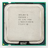
The final revision of the Pentium 4 was Cedar Mill, released on January 5, 2006. This was a die shrink of the Prescott-based 600 series core to 65 nm, with no real feature additions but significantly reduced power consumption. The Cedar Mill is closely linked to the Pentium D Presler revision, with each Presler CPU consisting of two Cedar Mill cores on the same chip package.[41] Cedar Mill had a lower heat output than Prescott, with a TDP of 86 W. The D0 stepping in late 2006 reduced this to 65 watts. It has a 65 nm core and features the same 31-stage pipeline as Prescott, 800 MT/s FSB, Intel 64, Hyper-Threading, but no Virtualization Technology. As with Prescott 2M, Cedar Mill also has a 2 MB L2 cache.
Intel initially announced four VT-x enabled Cedar Mill processors with model numbers 633 to 663,[42] but these were later cancelled and replaced by models 631 to 661 without VT-x, the extra 1 added to the model number distinguishing them from the 90 nm Prescott cores operating at the same frequencies.[43] Cedar Mill processors ranged in frequency from 3.0 to 3.6 GHz, down from the 3.8 GHz maximum of the Prescott-based 670 and 672. Overclockers managed to exceed 8 GHz with these processors using liquid nitrogen cooling.[44]
The name "Cedar Mill" refers to Cedar Mill, Oregon, an unincorporated community near Intel's Hillsboro, Oregon facilities.
Successor
[edit]In March 2003, the Pentium 4 M (the mobile version of the Pentium 4) was discontinued after suffering from heat and power consumption problems and was replaced by the P6-based Pentium M. The Pentium M forms a part of the Centrino platform-marketing brand throughout the 2000s.
In May 2005, Intel released dual-core processors under the Pentium D and Pentium Extreme Edition brands. These came under the code names Smithfield and Presler for the 90 nm and 65 nm parts respectively.
The original successor to the Pentium 4 was (codenamed) Tejas, which was scheduled for an early-mid-2005 release. However, it was cancelled a few months after the release of Prescott due to extremely high TDPs (a 2.8 GHz Tejas emitted 150 W of heat, compared to around 80 W for a Northwood of the same speed, and 100 W for a comparably clocked Prescott) and development on the NetBurst microarchitecture as a whole ceased, with the exception of the dual-core Pentium D, Pentium Extreme Edition and the Cedar Mill-based Pentium 4 HT.
The real successor to the Pentium 4 brand is the Pentium Dual-Core brand, released in 2006. The first chips implementing it (in 65 nm) were released in January 2007 with the Yonah mobile processors and are based on the Enhanced Pentium M architecture, in June 3, 2007 with the Allendale (and later Conroe) desktop processors and in late 2007 with the Merom mobile processors, with the underlying microarchitecture being the Core microarchitecture.
See also
[edit]- Intel Celeron (NetBurst-based)
- List of Intel Pentium processors
- List of Intel Pentium 4 processors
- List of Intel processors
Notes and references
[edit]- ^ "Product Change Notification, 107779 - 00" (PDF). Intel. 2007.
- ^ "Product Change Notification, 107779 - 00" (PDF). Intel. 2007.
- ^ Carmean, Doug (Spring 2002). "The Intel® Pentium® 4 Processor" (PDF).[self-published source?]
- ^ "X-bit labs - Print version". www.xbitlabs.com. Archived from the original on March 6, 2016. Retrieved January 11, 2022.
- ^ "Intel Introduces The Pentium 4 Processor". Intel. Archived from the original on April 3, 2007. Retrieved August 14, 2007.
- ^ "Intel intros 3.0 GHz quad-core Xeon, drops Pentiums". TG Daily. Archived from the original on May 17, 2019. Retrieved May 17, 2019.
- ^ "Product Change Notification, 107779 - 00" (PDF). Intel. 2007.
- ^ "Intel to unify product naming scheme". DIGITIMES. August 6, 2007. Retrieved November 22, 2024.
- ^ "New Pentium 4 rejects Rambus memory". ZDNet.
- ^ "Intel Goes DDR - do We Really Care?". December 17, 2001.
- ^ "Review: Intel Pentium 4 CPU". www.dansdata.com.
- ^ "Yes, Netburst really was that bad: CPU architectures tested - PC Perspective". August 3, 2011.
- ^ a b Magee, Mike. "Pentium 4 platform renamed". www.theregister.com.
- ^ "Pentium 4 high risk strategy for Intel".
- ^ Shimpi, Anand Lal. "The future of Intel's manufacturing processes". www.anandtech.com.
- ^ a b Fog, Agner (May 2, 2017). The microarchitecture of Intel, AMD and VIA CPUs (PDF) (Report). Technical University of Denmark. Archived (PDF) from the original on March 28, 2017. Retrieved April 8, 2018.
- ^ Bob Bentley, Intel, at DAC '01: Proceedings of the 38th annual Design Automation Conference, June 2001, ISBN 1581132972, pages 244-248 doi:10.1145/378239, paper conference reference
- ^ Anand Lal Shimpi (November 20, 2000). "Intel Pentium 4 1.4GHz & 1.5GHz". Anandtech.
- ^ a b Scott Wasson (September 10, 2001). "The Pentium 4 gets SDRAM: Two new chipsets". Tech Report.
- ^ Wasson, Scott. AMD's Athlon XP 1800+ processor, Tech Report, October 9, 2001.
- ^ a b Wasson, Scott and Brown, Andrew. Pentium 4 'Northwood' 2.2 GHz vs. Athlon XP 2000+, January 7, 2002.
- ^ Wasson, Scott. AMD's Athlon XP 2800+ and NVIDIA's nForce2, Tech Report, October 1, 2002.
- ^ Wasson, Scott. Intel's Pentium 4 3.2 GHz processor, Tech Report, June 23, 2003.
- ^ Wasson, Scott. AMD's Athlon XP 3200+ processor, Tech Report, May 13, 2003.
- ^ Shilov, Anton. Sudden Overclocked Northwood Death Syndrome. Is It Strange That Overclocked CPUs Eventually Die? Archived 2007-12-31 at the Wayback Machine, X-bit Labs, December 6, 2002.
- ^ "Mobile Intel Pentium 4 Processor-M Datasheet". Intel Corp.
- ^ "Intel's Mobile Pentium 4". Intel Corp.
- ^ Case, Loyd (January 30, 2004). "Review: Intel Prescott Pentium 4 Processor - Page 7 of 15 - ExtremeTech". Extremetech.
- ^ Smith, Tony. "Intel Pentium 4 Extremely Expensive Edition to ship Monday". www.theregister.com.
- ^ "Intel's Pentium 4 Prescott processor". The Tech Report. February 2, 2004. Retrieved August 28, 2007.
- ^ Pentium 4 Prescott 3GHz w/1MB L2 cache question, HardForum, March 7, 2004, retrieved April 23, 2020
- ^ CPU Heat Comparison: How Hot is Prescott?, AnandTech, April 16, 2004, retrieved January 8, 2012
- ^ Intel Pentium 4 Processor supporting HT Technology 3.40E GHz, ARK.Intel.com, February 2, 2004, retrieved December 15, 2012
- ^ a b c d Glaskowsky, Peter N. (2 February 2004). "Prescott Pushes Pipelining Limits". Microprocessor Report.
- ^ "Intel Says No to 64-bit Pentium 4 in Retail". XBitLabs. Archived from the original on June 3, 2004. Retrieved May 8, 2022.
- ^ IT Infrastructure – Intel Resources for IT Managers, Intel.com, retrieved January 8, 2012
- ^ "Intel CPU Roadmap Update". AnandTech. February 21, 2005. Retrieved May 8, 2022.
- ^ "Twice the Cache - 17% Higher Latency". AnandTech. October 27, 2004. Retrieved May 8, 2022.
- ^ "Intel Pentium 4 Processor 662 supporting HT Technology (2M Cache, 3.60 GHz, 800 MHz FSB)". Product Specifications. Intel.
- ^ "Intel Pentium 4 Processor 672 supporting HT Technology (2M Cache, 3.80 GHz, 800 MHz FSB)". Product Specifications. Intel.
- ^ "Intel to add Enhanced SpeedStep to 65nm desktop chips". The Register. February 1, 2006. Retrieved May 10, 2022.
- ^ "Intel On the Offensive: Roadmap Details and Analysis". AnandTech. June 14, 2005. Retrieved May 10, 2022.
- ^ "Intel's 65nm Gameplan: Presler and Cedar Mill Updates". AnandTech. September 9, 2005. Retrieved May 10, 2022.
- ^ "OC Team Italy sets a new world record at 8GHz". NordicHardware. January 22, 2007. Archived from the original on May 26, 2008. Retrieved January 11, 2008.
External links
[edit]- "The future of Prescott: when Moore gives you lemons..." at Ars Technica
- Prescott vs. Northwood Pentium 4 Review
- Intel Documentation
- Inside Pentium 4 Architecture
- The Microarchitecture of the Pentium 4 Processor
- P4 FPU's sensitive Denormalisation threshold and its effect on real-time audio processing Archived 2020-06-20 at the Wayback Machine


